- 您现在的位置:买卖IC网 > Sheet目录368 > W25Q40BWZPIG (Winbond Electronics)IC FLASH SPI 4MBIT 8WSON
�� �
�
�W25Q40BW�
�8.2.8�
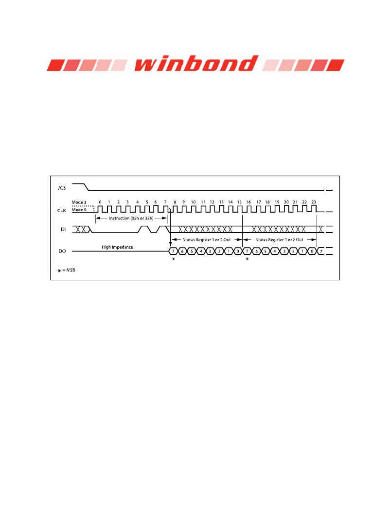
�Read� Status� Register-1� (05h)� and� Read� Status� Register-2� (35h)�
�The� Read� Status� Register� instructions� allow� the� 8-bit� Status� Registers� to� be� read.� The� instruction� is�
�entered� by� driving� /CS� low� and� shifting� the� instruction� code� “05h”� for� Status� Register-1� or� “� 35h� ”� for�
�Status� Register-2� into� the� DI� pin� on� the� rising� edge� of� CLK.� The� status� register� bits� are� then� shifted� out� on�
�the� DO� pin� at� the� falling� edge� of� CLK� with� most� significant� bit� (MSB)� first� as� shown� in� figure� 7.� The� Status�
�Register� bits� are� shown� in� figure� 3a� and� 3b� and� include� the� BUSY,� WEL,� BP2-BP0,� TB,� SEC,� SRP0,�
�SRP1,� QE,� LB3-0,� CMP� and� SUS� bits� (see� Status� Register� section� earlier� in� this� datasheet).�
�The� Read� Status� Register� instruction� may� be� used� at� any� time,� even� while� a� Program,� Erase� or� Write�
�Status� Register� cycle� is� in� progress.� This� allows� the� BUSY� status� bit� to� be� checked� to� determine� when�
�the� cycle� is� complete� and� if� the� device� can� accept� another� instruction.� The� Status� Register� can� be� read�
�continuously,� as� shown� in� Figure� 7.� The� instruction� is� completed� by� driving� /CS� high.�
�Figure� 7.� Read� Status� Register� Instruction� Sequence� Diagram�
�8.2.9�
�Write� Status� Register� (01h)�
�The� Write� Status� Register� instruction� allows� the� Status� Register� to� be� written.� Only� non-volatile� Status�
�Register� bits� SRP0,� SEC,� TB,� BP2,� BP1,� BP0� (bits� 7� thru� 2� of� Status� Register-1)� and� CMP,� LB3,� LB2,�
�LB1,� LB0,� QE,� SRP1� (bits� 14� thru� 8� of� Status� Register-2)� can� be� written� to.� All� other� Status� Register� bit�
�locations� are� read-only� and� will� not� be� affected� by� the� Write� Status� Register� instruction.� LB3-0� are� non-�
�volatile� OTP� bits,� once� it� is� set� to� 1,� it� can� not� be� cleared� to� 0.� The� Status� Register� bits� are� shown� in�
�figure� 3� and� described� in� 10.1.�
�To� write� non-volatile� Status� Register� bits,� a� standard� Write� Enable� (06h)� instruction� must� previously� have�
�been� executed� for� the� device� to� accept� the� Write� Status� Register� Instruction� (Status� Register� bit� WEL�
�must� equal� 1).� Once� write� enabled,� the� instruction� is� entered� by� driving� /CS� low,� sending� the� instruction�
�code� “01h”,� and� then� writing� the� st� atus� register� data� byte� as� illustrated� in� figure� 8.�
�To� write� volatile� Status� Register� bits,� a� Write� Enable� for� Volatile� Status� Register� (50h)� instruction� must�
�have� been� executed� prior� to� the� Write� Status� Register� instruction� (Status� Register� bit� WEL� remains� 0).�
�However,� SRP1� and� LB3,� LB2,� LB1,� LB0� can� not� be� changed� from� “1”� to� “0”� because� of� the� OTP�
�protection� for� these� bits.� Upon� power� off,� the� volatile� Status� Register� bit� values� will� be� lost,� and� the� non-�
�volatile� Status� Register� bit� values� will� be� restored� when� power� on� again.�
�-� 22� -�
�发布紧急采购,3分钟左右您将得到回复。
相关PDF资料
W25Q64BVSFIG
IC SPI FLASH 64MBIT 16SOIC
W25Q64CVZEIG
IC SPI FLASH 64MBIT 8WSON
W25Q64DWZEIG
IC FLASH SPI 64MBIT 8WSON
W25Q64FVSFIG
IC SPI FLASH 64MBIT 16SOIC
W25Q80BVSNIG
IC SPI FLASH 8MBIT 8SOIC
W25Q80BWSSIG
IC FLASH SPI 8MBIT 8SOIC
W25X40BVZPIG
IC SPI FLASH 4MBIT 8WSON
W25X64VZEIG
IC FLASH 64MBIT 75MHZ 8WSON
相关代理商/技术参数
W25Q40BWZPIG TR
制造商:Winbond Electronics Corp 功能描述:IC FLASH 4MBIT 80MHZ 8WSON
W25Q40BWZPIP
制造商:WINBOND 制造商全称:Winbond 功能描述:1.8V 4M-BIT SERIAL FLASH MEMORY WITH DUAL AND QUAD SPI
W25Q40CLSNIG
功能描述:IC FLASH SPI 4MBIT 8SOIC RoHS:是 类别:集成电路 (IC) >> 存储器 系列:SpiFlash® 标准包装:2,000 系列:- 格式 - 存储器:RAM 存储器类型:SRAM - 异步 存储容量:256K (32K x 8) 速度:15ns 接口:并联 电源电压:3 V ~ 3.6 V 工作温度:-40°C ~ 85°C 封装/外壳:28-TSSOP(0.465",11.8mm 宽) 供应商设备封装:28-TSOP 包装:带卷 (TR) 其它名称:71V256SA15PZGI8
W25Q40CLZPIG
功能描述:IC FLASH SPI 4MBIT 8WSON RoHS:是 类别:集成电路 (IC) >> 存储器 系列:SpiFlash® 标准包装:2,000 系列:- 格式 - 存储器:RAM 存储器类型:SRAM - 异步 存储容量:256K (32K x 8) 速度:15ns 接口:并联 电源电压:3 V ~ 3.6 V 工作温度:-40°C ~ 85°C 封装/外壳:28-TSSOP(0.465",11.8mm 宽) 供应商设备封装:28-TSOP 包装:带卷 (TR) 其它名称:71V256SA15PZGI8
W25Q64BV
制造商:WINBOND 制造商全称:Winbond 功能描述:64M-BIT SERIAL FLASH MEMORY WITH DUAL AND QUAD SPI
W25Q64BVDAIG
制造商:WINBOND 制造商全称:Winbond 功能描述:64M-BIT SERIAL FLASH MEMORY WITH DUAL AND QUAD SPI
W25Q64BVDAIP
制造商:WINBOND 制造商全称:Winbond 功能描述:64M-BIT SERIAL FLASH MEMORY WITH DUAL AND QUAD SPI
W25Q64BVSFIG
功能描述:IC SPI FLASH 64MBIT 16SOIC RoHS:是 类别:集成电路 (IC) >> 存储器 系列:SpiFlash® 标准包装:72 系列:- 格式 - 存储器:RAM 存储器类型:SRAM - 同步 存储容量:4.5M(256K x 18) 速度:133MHz 接口:并联 电源电压:3.135 V ~ 3.465 V 工作温度:0°C ~ 70°C 封装/外壳:100-LQFP 供应商设备封装:100-TQFP(14x20) 包装:托盘